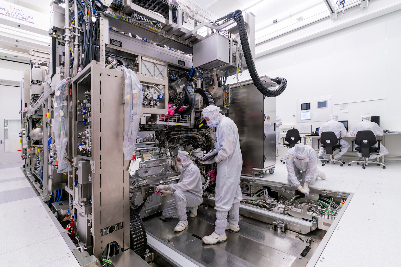
Chips are everywhere – most modern technology relies on them to the extent that most of us cannot even imagine a world without semiconductors. Just think of modern cars, phones, household appliances. The technology required to manufacture those chips is pushing the boundaries of science to new and unchartered territory.
The long-term growth of the semiconductor industry is based on the principle that the energy, cost and time required for electronic computations can be reduced by shrinking the transistors on microchips. One of the main “drivers of shrink” is the density – and hence miniaturisation – of transistors on a chip, which depends on the smallest feature resolution that lithography systems can achieve.
Lithography resolution is mainly determined by the wavelength of the light used and the numerical aperture of the optics. A shorter wavelength – like a finer brush used for painting – can print smaller features. A larger numerical aperture can focus the light more tightly, which also leads to better resolution. Building lithography machines has been an innovation challenge from the beginning.
Painting with the finest brush
ASML is a global innovation leader in the chip industry and provides chipmakers with hardware, software and services to mass produce patterns on silicon through lithography. Our lithography machines are not one innovation – they bring together countless innovations by us and our suppliers, each pushing the envelope on what can be technically achieved to obtain maximum precision.
To keep moving the needle in enabling ever faster and less energy-intensive microchips, we have to relentlessly drive our technology forward. When we set out to develop the latest generation of lithography machines capable of the highest resolution, we had to learn how to harness light with an extremely short wavelength – Extreme Ultra Violet (EUV) light. This was pioneering work in many respects and all in all, it took well over a decade of tenacity to get our EUV technology off the ground.
The tricky thing with harnessing EUV light for lithography is that it is absorbed by everything, even air. That is why our EUV system has a large vacuum chamber in which the light can propagate far enough to land on the wafer. The light is guided by a series of ultra-reflective mirrors, made by our German partner ZEISS SMT. These mirrors are so smooth that, if they were to be scaled to the size of Germany, the biggest bump would be less than a millimeter high.
And EUV light is also notoriously hard to generate. Our EUV system uses a high energy 30-kilowatt laser that fires on a microscopic droplet of molten tin 50,000 times per second, turning it into plasma that emits the EUV light, which then is focused into a uniform beam.
EUV lithography is now being used by the world’s largest logic and memory chipmakers. We continue to push the roadmap for this technology for years to come, delivering systems with higher productivity and better imaging performance. These advances in lithography enable the industry to continue increasing the value and lower the cost of a chip – setting a basis for innovation in many other goods (e.g. phones) that become affordable for many more people.

An ASML ecosystem
We could never have achieved this alone – so we have learned to rely on others, too. For this we tap into the collective knowledge of our global ecosystem across suppliers, academic partners, customers and peers. Our ecosystem approach has led customers to co-investing in EUV with us, as well as a renewed partnership model with ZEISS SMT, our trusted partner for optics. We have also made acquisitions that boosted our capabilities across our product portfolio.
As a company we foster an environment where people can contribute, learn and grow, because we believe our purpose is to unlock the potential of people and society by pushing technology to new limits. But we also know that innovation is rarely a straight line. It takes laser focus, multidisciplinary teamwork and a keen eye for how we can best help our customers. And even then, we have had to show resilience.
Why Europe?
There are various reasons why ASML could be created in Europe – or more specifically in Veldhoven in The Netherlands, but the most important one is the European willingness to cooperate and share risks and rewards. This holds true for cooperations between companies, universities, governments and research and technology organisations.
The EU internal market and the collaborative spirit between system integrators and technology suppliers in the EU is what has made ASML a success story and it has brought many SMEs/startups across Europe to the next stage, employing thousands rather than dozens.
Europe has what it takes to build and maintain technological leadership – and Europe benefits from this. The innovations that our technology enables are key to develop solutions for our own continent: renewable energy, health, new modes of transport, education, (tele)communication and new forms of computing. And yet, without reliable access to state-of-the-art equipment, a chip production ramp-up would become much harder to achieve, leaving the fate of European industries increasingly in the hands of third countries.
Excellence in advanced semiconductor equipment and production process development provides us with global leverage in a world which is breaking up into socio-economic blocks. The technology that we at ASML enable has become of strategic importance – to the extent that semiconductor technology is now posing challenges for our trade relationships. Innovation has dealt us strong cards which, if we use them wisely will contribute to Europe’s strategic autonomy and place in the world.

